Optimal Component Arrangement
We position components to minimize trace lengths, reduce parasitics, and optimize performance for both high-speed and analog circuits.
We position components to minimize trace lengths, reduce parasitics, and optimize performance for both high-speed and analog circuits.
Our team accounts for thermal management, heat dissipation, and mechanical constraints, ensuring reliable and durable PCB operation.
Component placement is organized for accessibility, testing, and maintenance, making boards more reliable and easier to service.
Controlled impedance, differential pair routing, and careful signal path planning to ensure signal integrity for fast digital and RF circuits.
Optimized routing of power and ground planes to reduce noise, voltage drop, and improve overall electrical performance.
Expert handling of multi-layer boards, stack-up planning, and routing strategies to maximize performance while minimizing crosstalk and EMI.
Our team has extensive experience in component placement and routing for ATE boards, high-speed digital, analog, and power electronics.
We tailor the placement and routing approach for each project, balancing performance, manufacturability, and thermal requirements.
Every trace, via, and pad is optimized to meet performance and reliability goals, with careful planning for high-density and fine-pitch designs.
Our layout engineers collaborate closely with schematic and test teams to ensure seamless integration and efficient production.
Examples of PCB layout & tools we use.
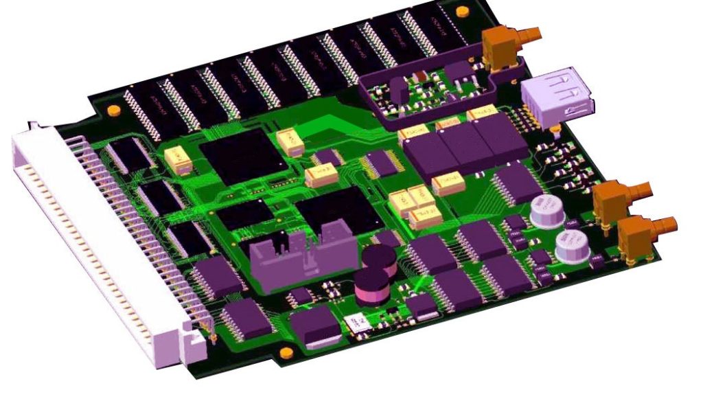
Rendering & layout review.
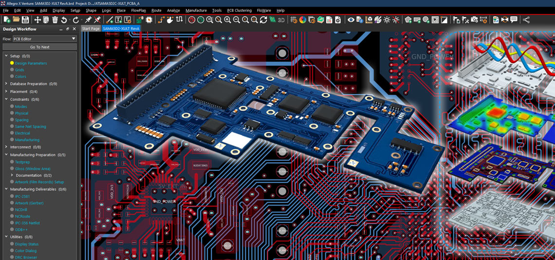
Modern PCB design flow.
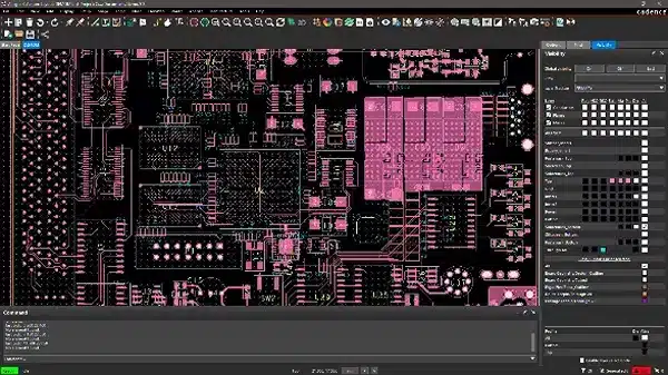
Placement & routing tools.
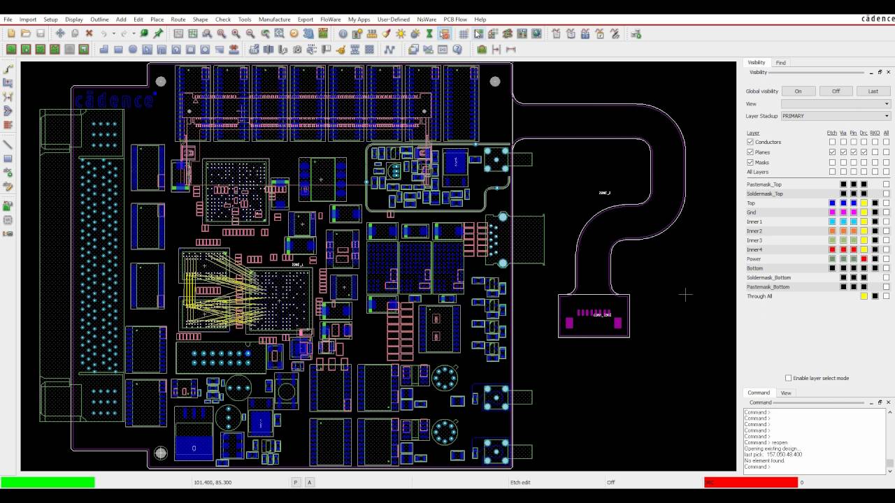
High-density routing.
Send us your requirements and we’ll propose the best placement & routing strategy for your project.
Get in Touch